L1 Implementation

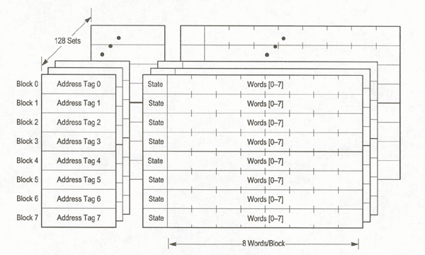
Above is a diagram of the L1 organization.
Here, in the MPC7400 model of the G4 processor, instruction and data caches are separate. Each cache is 32-Kbye and 8-way set associative. Note, each cache block contains eight contigous words from memory that are loaded fom an 8-word boundary. Thus, a cache block never crosses a page boundary. This provides performance benefits since misaligned accesses across a page boundary can incur penalties.
L2 Implementation
The L2 cache is unified cache. It is implemented as an on-chip, two-way, set-associative tag memory with external, sychronous SRAMs for data storage. These external SRAMs are accessed through a dedicated L2 cache port. The port will support a single bank 512-Kbyte, 1-Mbyte, or 2-Mbyte synchronous SRAMs.
Organization of the L2 cache depends on the size. The cache can be organized in 32-, 64-, or 128 bye lines. Lines are subdivided into 32-byte blocks.
The L2 cache receives requests from both L1 instruction and data caches. Multiple and simultaneous accesses are both supported. Thus it is possible to process L1 instruction cache and L2 data cache requests at the same time. The L1 data cache requests are handled by data the reload table. Requests from L1 cache generally result from instruction misses, data load or store misses. Requests from L1 cache are looked up in L2 tags and serviced if they are a hit, otherwise the request if forwared further to the bus interface if they miss.