|
|
|
|
|
|
|
|
|
|
|
|
|
|
|
Memory: chip enable |
|
|
|
|
|
|
|
Need to generate signals
to determine which addresses to access in memory |
|
|
Logic for chip enable |
|
|
|
|
CPU can generate 3
control signals: |
|
|
|
|
B which indicates that
the CPU wants to access a byte |
|
|
|
|
H which indicates that
the CPU wants to access a halfword |
|
|
|
|
W which indicates that
the CPU wants to access a word |
|
|
|
|
Which chips are enabled? |
|
|
|
|
|
|
B: 1 chip |
|
|
|
|
|
|
H: 2 chips |
|
|
|
|
|
|
W: all 4 chips |
|
|
|
|
|
|
Address patterns: |
|
|
|
|
addresses on chip 00 end
in 00 (divisible by 4) |
|
|
|
|
|
addresses on chip 01 end
in 01 (congruent to 1 mod 4) |
|
|
|
|
addresses on chip 10 end
in 10 (congruent to 2 mod 4) |
|
|
|
|
addresses on chip 11 end
in 11 (congruent to 3 mod 4) |
|
|
|
|
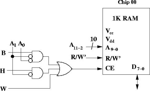
Logic for chip 00: |
|
|
|
|
If W = 1, then all four
chips are enabled |
|
|
|
|
|
If B = 1, select chip 00
when A1A0 = 00 |
|
|
|
|
If H = 1, select Chip 00
if A1 = 0 (already know
that A0 = 0) |
|
|
|
|
Boolean expression: |
|
|
|
|
CE = W + (H * A1') + (B * A1'A0') |
|
|
|
|
|

|
|
|
|
|
|
|
|
|
|
|
|
|
|
|
|
|
|
|
|
|
|
|
|
|
|
|
|
|
|
|
|
|
|
|
|
|
|
|
|
|
|
|
|
|
|
|
|
|
|
|
|
|
|
|
|
|
|
|
Notice address bits A9-0: |
|
|
|
|
To get M[i], access index
i / 4 |
|
|
|
Same as shifting to the
right by 2 bits, or accessing bits 11-2 from the address bus |
|
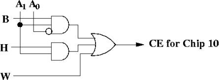
Chip 10: |
|
|
|
|
|
CE = W + (H * A1) + (B * A1A0') |
|
|
|
|

|
|
|
|
|
|
|
|
|
|
|
|
|
|
|
|
|
|
|
|
|
|
|
|
|
|
|
|
|
Invalid addresses: |
|
|
|
|
|
we assume that the other
20 bits of the address are all 0 |
|
|
|
|
|
|
|
|
|
|
|
|
|
|
|
|
|
|
|
|
