|
|
|
|
|
|
|
|
|
|
|
|
|
|
|
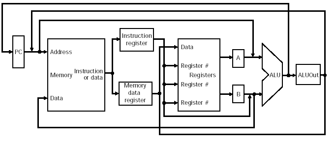
Multi-cycle datapath |
|
|
|
|
|
|
|
Multi-cycle
implementaion: break up instructions into separate steps |
|
|
|
|
Each step takes a single
clock cycle |
|
|
|
|
Each
functional unit can be used more than once in an instruction, |
|
|
|
|
as long as it is used in
different clock cycles |
|
|
|
|
Reduces amount of
hardware needed |
|
|
|
|
Reduces average
instruction time |
|
|
|
|
|
Differences with
single-cycle |
|
|
|
|
|
|
|
Single memory for
instructions and data |
|
|
|
|
|
Single ALU (no separate
adders for PC or branch calculation) |
|
|
|
|
Extra registers added
after major functional units to hold results between clock cycles |
|
|
|
|
|
|
|
|
|
|
|
|
|
|
|
|
|
|
|
|
|
|
|
|
|
|
|
|
|
|
|
|
|
|
|
|
|
|
|
|
|
|
|
|
|
|
|
|
|
|
|
|
|
|
|
|
|
|
|
|
|
|
|
|
Fig. 5.30 |
|
|
|
|
|
|
|
|
Note
that data needed in a later instruction must be in one of the |
|
|
|
|
programmer-visible
registers or memory |
|
|
|
|
Assume each clock cycle
includes at most one of: |
|
|
|
|
Memory access |
|
|
|
|
Register file access (2
reads OR 1 write) |
|
|
|
|
ALU operation |
|
|
|
|
Any data produced from 1
of these 3 functional units must be stored between cycles |
|
Instruction register: contains current instruction |
|
|
|
|
Memory data register: data from main memory |
|
|
|
|
Why 2 separate
registers? Because both values are
needed simultaneously |
|
Register output A, B |
|
|
|
|
2 operand values read
from register file |
|
|
|
|
ALUOut |
|
|
|
|
|
Output from ALU |
|
|
|
|
|
Why
is this needed? Because we are
combining adders into the ALU, |
|
|
|
so we need to select
where the output goes (register file or memory) |
|
All
these registers except IR hold data only between consecutive clock cycles, |
|
|
|
so don't need write
control signal |
|
|
|
|
What else do we need? |
|
|
|
|
Because functional units
are used for multiple purposes: |
|
|
|
More MUXes |
|
|
|
More inputs for existing
MUXes |
|
|
|
|
|
|
|
|
|
|
|
|
|
|
|
|
|
|
|
|
|
|
|
|